Industrial Wafer Manufacturing Machines: Process and Equipment Guide
Industrial wafer manufacturing machines are specialized systems used to transform semiconductor-grade materials, particularly silicon, into precisely engineered wafers. These wafers form the foundation on which integrated circuits, memory devices, sensors, power electronics, and other semiconductor components are manufactured.
The wafer production process begins with high-purity semiconductor material. In silicon wafer manufacturing, purified silicon is commonly formed into a single-crystal ingot. The ingot is then processed into thin circular wafers through several controlled mechanical and chemical operations.
A typical wafer manufacturing sequence can include:
- Crystal growth and ingot formation
- Ingot shaping and diameter control
- Wafer slicing
- Edge grinding
- Surface grinding
- Lapping or polishing
- Chemical cleaning
- Surface treatment
- Dimensional measurement
- Defect inspection
- Final packaging and handling
Industrial wafer manufacturing machines are designed to maintain extremely precise process conditions. Small variations in thickness, flatness, surface roughness, contamination, or crystal quality can affect later semiconductor manufacturing steps.
The equipment used for wafer production is different from the equipment used to manufacture the complete semiconductor device. Wafer manufacturing prepares the substrate, while semiconductor fabrication subsequently creates electronic structures on that substrate.
The broader semiconductor manufacturing environment includes hundreds of specialized equipment types for processes such as deposition, lithography, etching, implantation, cleaning, and packaging.
Importance
The importance of industrial wafer manufacturing machines has increased as semiconductor technology has expanded into artificial intelligence, data centers, automotive electronics, telecommunications, industrial automation, medical electronics, and consumer devices.
A high-quality wafer provides a controlled foundation for subsequent semiconductor processing. Consistent wafer geometry and surface characteristics can help fabrication facilities maintain process stability across large numbers of wafers.
Several areas make wafer manufacturing particularly important.
Precision and dimensional control
Modern semiconductor production requires carefully controlled wafer thickness, diameter, flatness, and surface characteristics. Automated measurement equipment helps identify deviations before wafers move to later manufacturing stages.
Surface quality
The wafer surface must be sufficiently smooth and clean for advanced semiconductor processes. Grinding, polishing, cleaning, and inspection equipment therefore play important roles in preparing the substrate.
Manufacturing consistency
Industrial equipment allows repeated processing under defined conditions. Automation can also reduce variation between production batches and improve process monitoring.
Advanced semiconductor demand
The semiconductor industry is experiencing strong growth associated with AI infrastructure, advanced computing, communications, transportation, and industrial technologies. The Semiconductor Industry Association reported that global semiconductor sales reached $403.3 billion in Q2 2026, representing a 35.1% increase from Q1.
For manufacturers, this broader expansion increases the importance of reliable wafer production capacity and advanced semiconductor manufacturing equipment.
| Wafer Manufacturing Stage | Typical Equipment | Main Purpose |
|---|---|---|
| Crystal growth | Crystal growth furnace | Produces semiconductor ingots |
| Ingot shaping | Diameter grinding system | Controls ingot dimensions |
| Wafer slicing | Wire saw | Cuts ingots into wafers |
| Edge processing | Edge grinder | Shapes and strengthens wafer edges |
| Surface grinding | Wafer grinder | Controls thickness and flatness |
| Polishing | CMP/polishing system | Produces smooth wafer surfaces |
| Cleaning | Wafer cleaning equipment | Removes particles and residues |
| Inspection | Optical inspection system | Detects surface defects |
| Measurement | Metrology equipment | Measures critical dimensions |
Recent Updates
Semiconductor manufacturing has continued to expand rapidly during 2026. A July 2026 industry report stated that global semiconductor sales reached a record $795.6 billion in 2025, while worldwide sales were projected to reach approximately $1.5 trillion in 2026. The report connected this growth with AI, advanced computing, communications, healthcare, transportation, and other semiconductor applications.
This growth is influencing wafer manufacturing in several ways.
Greater automation
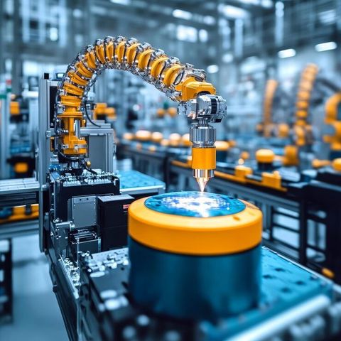
Manufacturing facilities increasingly integrate automated wafer handling, robotics, process monitoring, and equipment-control systems. Automation helps maintain repeatability while reducing unnecessary manual handling.
Advanced process monitoring
Modern wafer production increasingly depends on metrology and inspection technologies capable of identifying very small variations. Data from these systems can be used to monitor production conditions and detect process drift.
Equipment integration
Manufacturers are increasingly connecting individual machines with factory-level control and data systems. This enables better tracking of wafer movement, equipment status, process conditions, and production data.
Environmental improvements
Semiconductor manufacturing uses specialized gases, chemicals, and other materials. Environmental management has therefore become an important part of equipment development. EPA notes that semiconductor processes use fluorinated compounds for applications such as plasma etching and chamber cleaning, and the industry has implemented approaches intended to reduce associated greenhouse-gas emissions.
Expansion of manufacturing capacity
The 2026 semiconductor industry outlook also reflects significant investment in semiconductor manufacturing infrastructure. The SIA reported that companies had announced more than $770 billion in private-sector semiconductor investments in the United States since 2020 across 160 projects in 30 states.
These developments can increase demand for wafer-processing equipment, factory automation, metrology, cleanroom infrastructure, materials handling, and process-control technologies.
Laws and Policies
Regulatory requirements vary by country and depend on the manufacturing process, chemicals used, facility size, emissions, wastewater, worker protection, and environmental conditions.
In the United States, semiconductor manufacturing is subject to environmental requirements covering hazardous air pollutants. The U.S. Environmental Protection Agency's semiconductor NESHAP framework covers activities from crystal growth through wafer fabrication, testing, and assembly.
Air-quality considerations are particularly important because semiconductor manufacturing can involve substances such as hydrogen fluoride, hydrochloric acid, methanol, xylene, and glycol ethers.
Greenhouse-gas reporting can also apply to qualifying electronics manufacturing facilities. EPA's Subpart I framework establishes reporting requirements for facilities that meet the applicable source-category and reporting thresholds.
Chemical restrictions can also affect semiconductor manufacturing equipment and materials. In 2026, EPA updated certain requirements affecting persistent, bioaccumulative, and toxic chemicals, including provisions relevant to some manufacturing equipment used in semiconductor production.
Another recent development concerns refrigerants and process cooling. In May 2026, EPA published a reconsideration rule involving technology-transition requirements, including industrial process refrigeration and chillers used in semiconductor manufacturing.
Outside the United States, manufacturers need to follow the applicable environmental, chemical, occupational-safety, energy, waste-management, and semiconductor-industry regulations in their respective jurisdictions.
Tools and Resources
Several categories of tools can help engineers, students, researchers, and manufacturing professionals understand wafer production.
Process-flow diagrams
These help visualize the sequence from semiconductor crystal growth to wafer slicing, polishing, cleaning, inspection, and final preparation.
Wafer measurement calculators
Thickness, diameter, flatness, material-removal rates, and dimensional calculations can be useful when studying wafer-processing requirements.
Equipment monitoring systems
Industrial monitoring platforms can track temperature, pressure, vibration, chemical conditions, equipment status, and production parameters.
Metrology tools
Optical measurement, surface analysis, thickness measurement, particle inspection, and defect-detection systems help evaluate wafer quality.
Manufacturing databases
Technical databases can provide information about semiconductor materials, process specifications, equipment categories, and manufacturing terminology.
Learning resources
Useful educational materials include semiconductor process guides, engineering textbooks, equipment manuals, technical glossaries, manufacturing diagrams, laboratory training materials, and regulatory documentation.
A useful learning approach is to study the complete wafer process rather than focusing on one machine. Understanding how slicing, grinding, polishing, cleaning, inspection, and metrology interact provides a clearer picture of industrial wafer manufacturing.
FAQs
What are industrial wafer manufacturing machines?
Industrial wafer manufacturing machines are specialized systems used to produce and prepare semiconductor wafers. They can perform operations such as crystal processing, slicing, grinding, polishing, cleaning, measurement, inspection, and handling.
What material is commonly used for semiconductor wafers?
Silicon is the most widely used semiconductor wafer material. Other materials, including silicon carbide and gallium nitride, are also important for particular applications such as power electronics and high-frequency devices.
Why is wafer polishing important?
Polishing creates a highly controlled wafer surface by removing surface irregularities and improving smoothness. A consistent surface is important for subsequent semiconductor manufacturing processes.
What is wafer metrology?
Wafer metrology involves measuring characteristics such as thickness, flatness, dimensions, surface properties, and other process parameters. It helps manufacturers identify variations and maintain process control.
Are wafer manufacturing machines the same as semiconductor fabrication equipment?
No. Wafer manufacturing machines prepare the semiconductor substrate, while fabrication equipment is used later to create electronic structures on the wafer through processes such as deposition, lithography, etching, and implantation.
Conclusion
Industrial wafer manufacturing machines are an essential part of the semiconductor supply chain. They transform high-purity semiconductor materials into precisely controlled wafers that can support advanced electronic-device manufacturing.